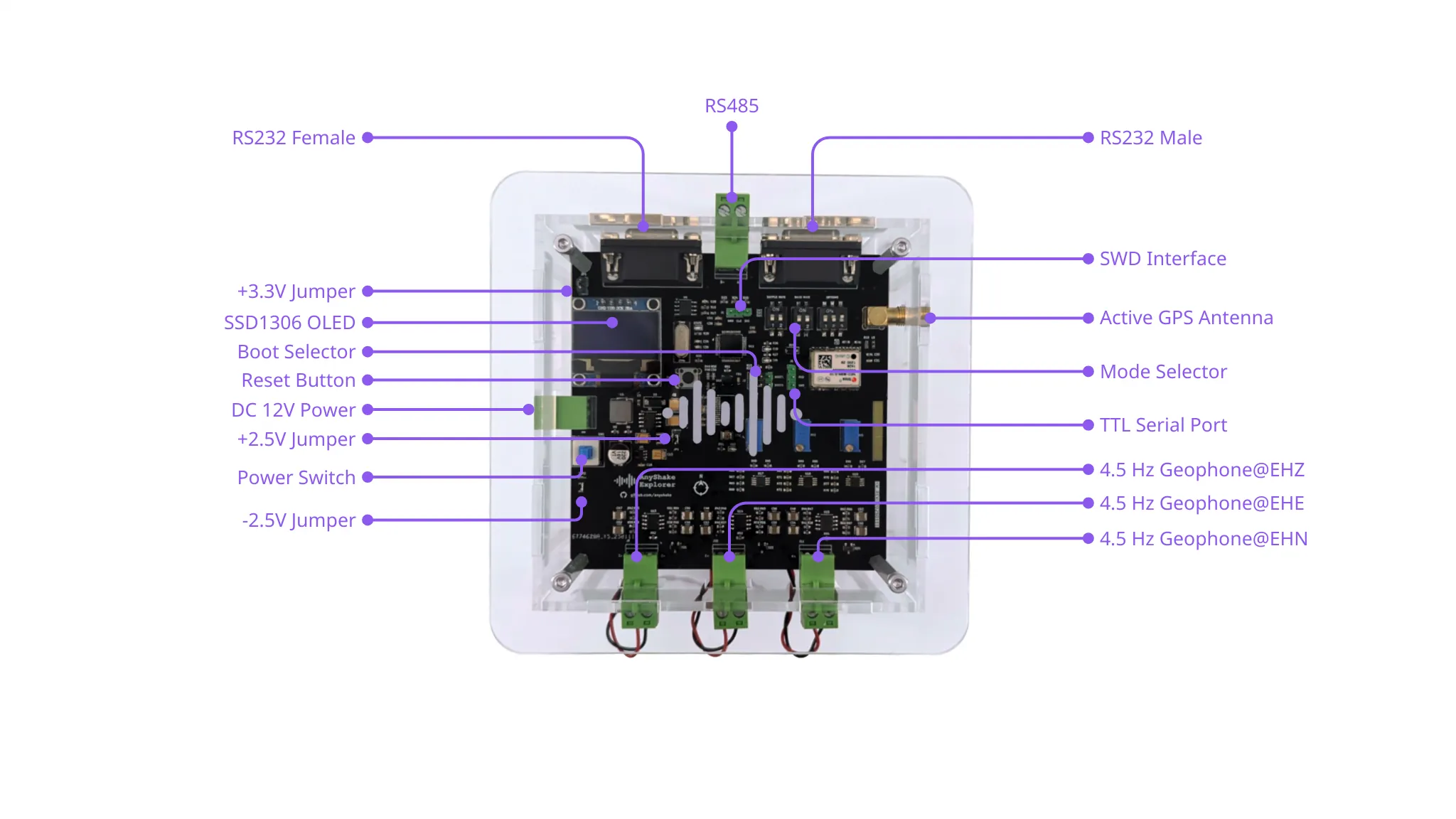
Hardware Interface
This section provides a comprehensive explanation of the hardware interfaces available on E-C111G. The following diagram illustrates the hardware interface:
Power Interface
Power Supply
The E-C111G operates on a DC power input ranging from 9 V to 12 V, delivered through a 2-pin terminal block or a DC barrel jack (available in newer hardware revisions). Internally, the input voltage is regulated to provide the multiple voltage rails required by the system: +3.3 V, +2.5 V, and −2.5 V.
The power input stage is robustly protected with:
- Overvoltage and short-circuit protection
- Reverse polarity protection
- A TVS (transient-voltage-suppression) diode to guard against input surges
The E-C111G is designed with energy efficiency in mind. Under normal operating conditions, its power consumption is approximately 0.6 W.
Power Control
The device includes an onboard self-locking push-button switch to control the main power. Pressing the switch powers on the system, and it remains latched until powered off.
To support development and diagnostics, three voltage rail control jumpers are provided:
JP1— Controls the +3.3 V rail, primarily used by digital logic (e.g., MCU, OLED)JP2— Controls the +2.5 V rail, typically used by analog components such as op-amps and ADCsJP3— Controls the −2.5 V rail, required for analog signal processing stages
All jumpers are closed by default, enabling full functionality. Developers may open them to isolate power rails during troubleshooting or measurement.
Test Points
To facilitate voltage verification during testing or development, the PCB includes clearly marked test points on the rear side:
| Test Point | Description | Typical Voltage |
|---|---|---|
TP4 | DC-DC output for analog subsystems | ~+5.5 V |
TP2 | Regulated analog reference | +2.5 V |
TP5 | Digital supply for MCU and peripherals | +3.3 V |
TP1 | Inverted DC-DC output (pre-regulator) | ~−5.0 V |
TP3 | Regulated negative analog rail | −2.5 V |
Power Architecture
The internal power architecture is illustrated below:
The system employs multiple regulators for improved stability and noise performance. Notably, analog and digital grounds are separated on the PCB to minimize high-frequency interference between subsystems. The two ground planes are connected via a 0 Ω resistor, allowing controlled return current flow while maintaining signal integrity.
Communication Ports
The E-C111G supports multiple serial communication protocols to accommodate diverse deployment scenarios. Each interface outputs identical real-time data streams, allowing simultaneous connection to multiple host systems such as PCs, embedded controllers, or industrial gateways.
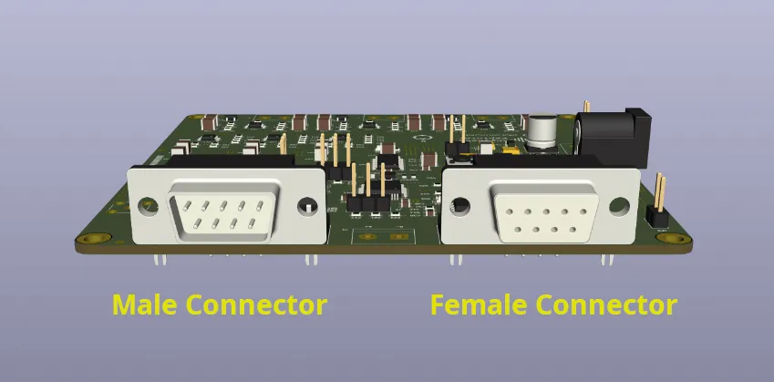
RS-232 Interface
The RS-232 interface uses industry-standard DB9 connectors, with both male and female ports available on the device.
- Connector Type: DB9 (1× male, 1× female)
- Voltage Level: ±12V (compliant with RS-232 standard)
- Maximum Baud Rate: 409600 bps
- Duplex Mode: Full-duplex
- Recommended Cable Length: Up to 10 m (depending on environment)
- Use Case: Ideal for direct serial connections to desktop computers, industrial PCs, or SBCs such as Raspberry Pi (via USB–RS232 adapters), offering mature driver support and excellent compatibility
The following figures illustrate the RS-232 connectors on E-C111G:
We recommend using the RS-232 interface in most scenarios due to its stability, simplicity, and broad compatibility across platforms.
RS-485 Interface
The RS-485 port is provided via a 2-pin screw terminal for direct connection to twisted-pair cabling. It supports differential half-duplex communication, making it suitable for longer cable runs and more electrically noisy environments.
- Connector Type: 2-pin terminal block (A/B)
- Voltage Level: 3.3V logic (via transceiver)
- Maximum Baud Rate: 115200 bps
- Duplex Mode: Half-duplex
- Termination & Biasing: External (user-supplied if required)
- Recommended Cable Length: Up to 50 m (at lower baud rates, using shielded twisted-pair)
- Use Case: Designed for industrial and long-distance applications, such as connecting remote sensors, outdoor enclosures
The following figure illustrates the RS-485 signal lines on E-C111G:
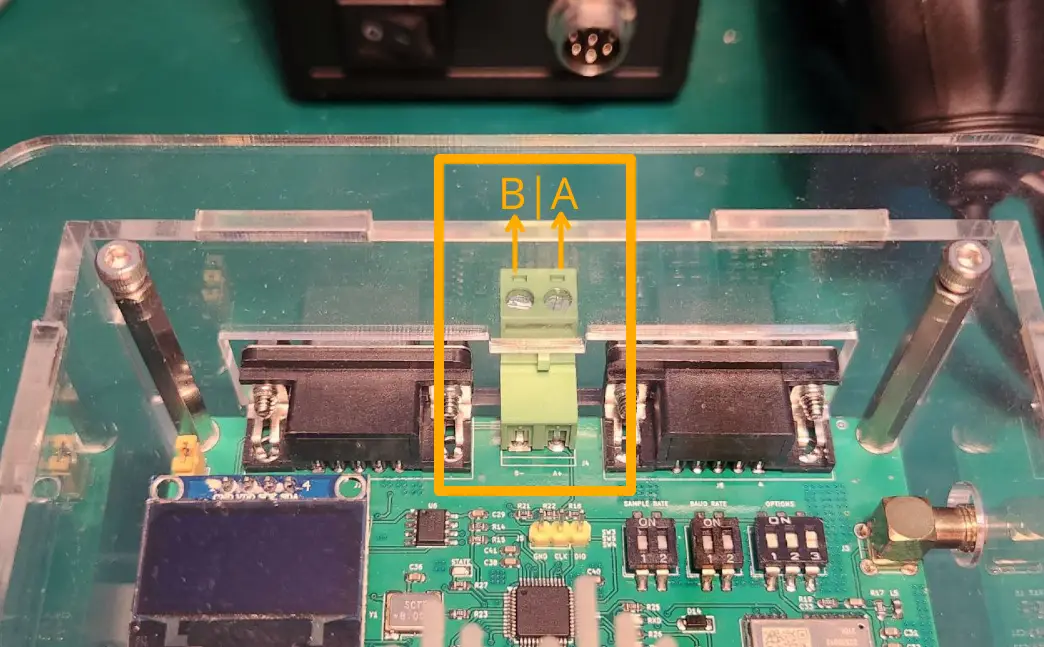
RS-485 wiring is not standardized. Ensure consistent signal lines (A/B) alignment across all devices on the bus.
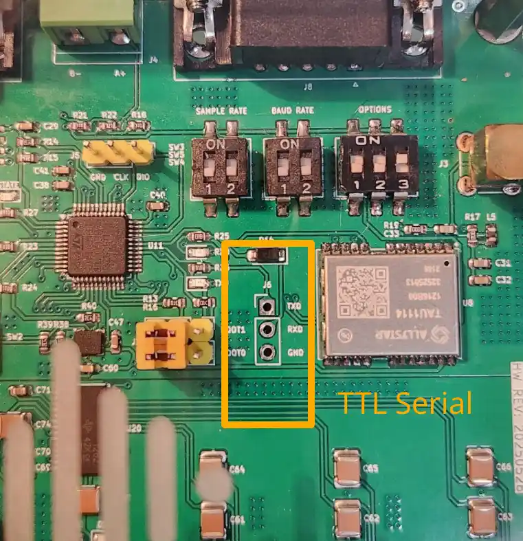
TTL Serial Interface
A 2.54mm 3-pin TTL-level UART header is provided for embedded system integration or firmware development. This interface operates at 3.3 V logic levels and is not electrically isolated, so careful attention must be paid during connection.
- Connector Type: 3-pin header (TX, RX, GND)
- Voltage Level: 3.3V logic (non-inverted)
- Maximum Baud Rate: 409600 bps
- Duplex Mode: Full-duplex
- Use Case: Recommended for embedded system development, including:
- Integration with SBC GPIOs
- Direct serial communication with microcontrollers (STM32, RP2040, etc.)
Connecting this port to 5V logic (e.g., older Arduino boards) may permanently damage the device. Always verify voltage compatibility before use.
Summary
| Interface | Connector Type | Logic Level | Max Baud Rate | Duplex | Typical Use Case |
|---|---|---|---|---|---|
| RS-232 | DB9 (male/female) | ±12V | 409600 bps | Full | General PC/server/SBC connection |
| RS-485 | 2-pin terminal | 3.3V diff. | 115200 bps | Half | Long-distance communication |
| TTL Serial | 3-pin header | 3.3V | 409600 bps | Full | SBC/microcontroller GPIO communication |
Debugging and Boot Configuration
The E-C111G firmware is fully open source and actively maintained. Users are encouraged to customize, compile, and flash the firmware to suit their specific use cases. The system supports field upgrades and includes a digital inclinometer mode, which enables users to access onboard accelerometer data for precise leveling and optimal sensor installation.
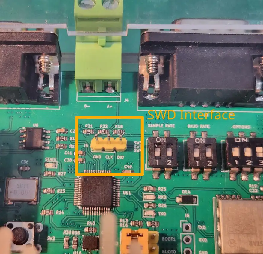
SWD Interface
The device provides a Serial Wire Debug (SWD) interface via a 3-pin 2.54 mm header, compatible with standard development tools such as ST-Link and J-Link.
GND— GroundSWDIO— Data I/OSWCLK— Clock
This interface allows for:
- Firmware flashing
- Breakpoint debugging
- Real-time memory inspection
The SWD interface is not electrically isolated. Use caution when connecting to a powered system to avoid potential damage to your programmer or the device.
For example, when using the official ST-Link V2 for SWD debugging, connect the pins as follows:
| ST-Link V2 Pin | E-C111G Pin |
|---|---|
| Pin 4 (GND) | GND |
| Pin 7 (SWDIO) | DIO |
| Pin 9 (SWCLK) | CLK |
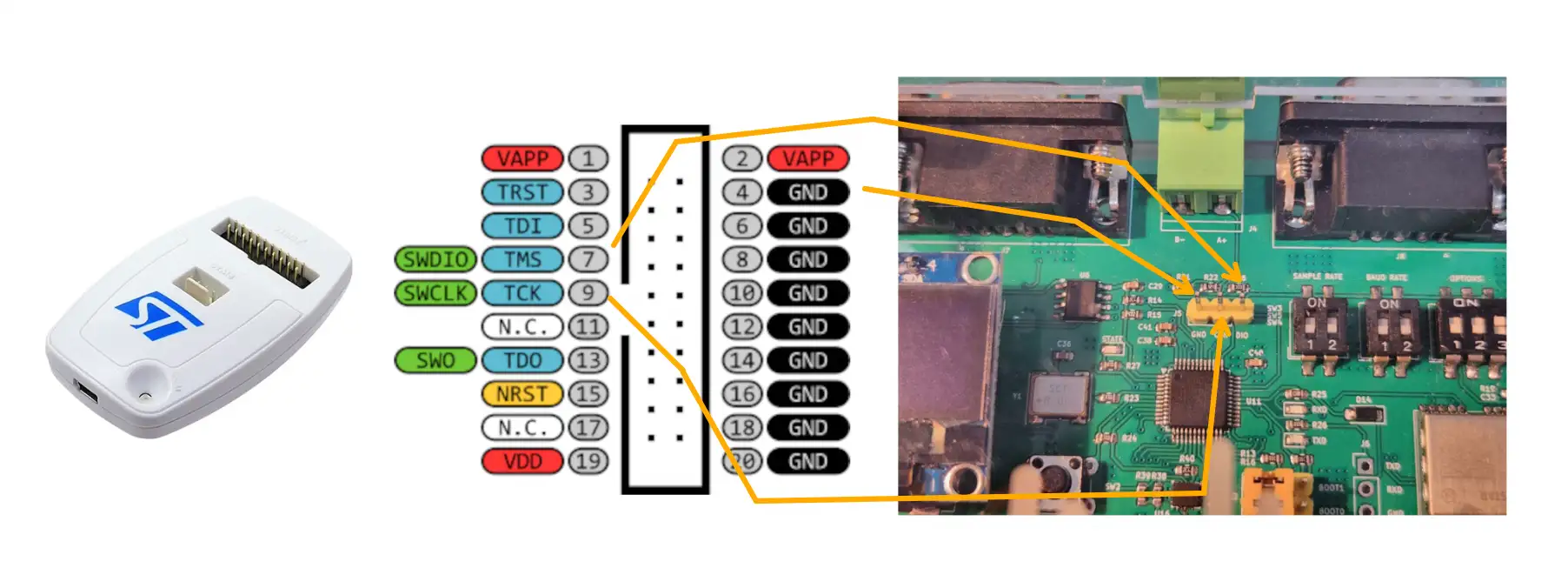
If you are using J-Link or other SWD-compatible tools, please refer to the vendor’s pinout documentation to ensure proper connection.
Boot Mode Selection
The E-C111G provides 4 boot modes selectable via a dual BOOT0/BOOT1 jumper configuration. These modes allow users to switch between normal operation, inclinometer mode, and firmware update modes.
| BOOT0 | BOOT1 | Boot Mode | Description |
|---|---|---|---|
| 0 | 0 | Main Flash (Acquisition) | Default mode; runs the primary firmware for seismic data acquisition. |
| 0 | 1 | Main Flash (Leveling) | Starts the firmware in inclinometer mode to assist with installation alignment. |
| 1 | 0 | System Memory | Enters STM32 built-in bootloader. |
| 1 | 1 | Embedded SRAM | Used for development and debugging temporary firmware loads. |
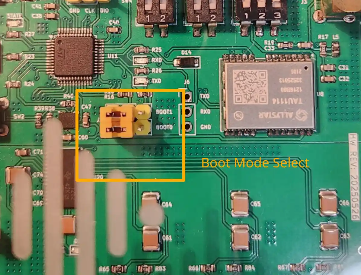
Boot mode is read on startup. After changing jumper positions, a manual reset is required to apply the new boot mode.
By default, the device boots from main flash (BOOT0=0, BOOT1=0) into seismic data acquisition mode.
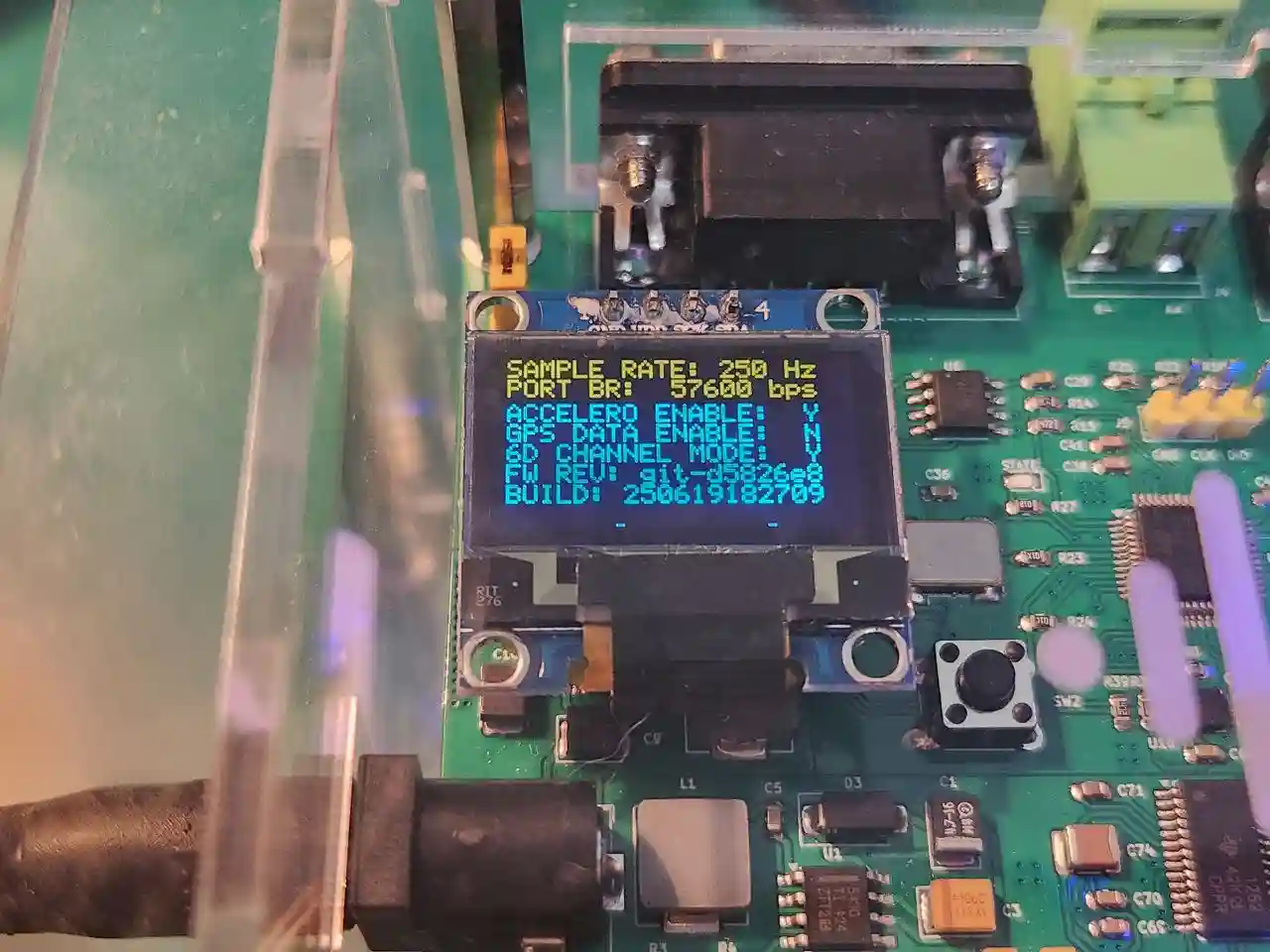
Mode Configuration and Display
The E-C111G supports multiple operating modes that can be configured using onboard DIP switches. A built-in 0.96-inch OLED display provides system status, connection information, making the setup process intuitive and efficient.
Sampling Rate Configuration
The sampling rate determines how frequently data is read from the sensors each second. It is configured via the SW3 DIP switch.
| Bit 1 | Bit 2 | Sample Rate | Notes |
|---|---|---|---|
| 0 | 0 | 250 SPS | Default setting |
| 0 | 1 | 200 SPS | |
| 1 | 0 | 100 SPS | |
| 1 | 1 | 50 SPS | For bandwidth-limited use |
The sampling rate directly affects the data resolution and system bandwidth. Higher rates provide finer temporal detail but require more storage and bandwidth.
Baud Rate Configuration
The baud rate defines the transmission speed of serial data. It is configured using the SW5 DIP switch.
| Bit 1 | Bit 2 | Baud Rate | Notes |
|---|---|---|---|
| 0 | 0 | 57600 | Default; best stability |
| 0 | 1 | 115200 | Common for USB–Serial adapters |
| 1 | 0 | 230400 | Faster transfer |
| 1 | 1 | 409600 | Maximum supported rate |
Lower baud rates offer more robust communication, especially over long cables or electrically noisy environments. Adjust this according to your host system’s capability.
Extended Mode Options
Additional features can be enabled via individual bits of the SW4 DIP switch. These allow for specialized data acquisition modes.
Accelerometer-Only Mode
- Control: Bit 1
- Function: Acquires data only from the onboard accelerometer, ignoring geophone input.
This bit is ignored when 6-channel mode is enabled.
GNSS Synchronization
-
Control: Bit 2
-
Function: Enables GNSS synchronization at startup.
-
Startup Condition:
- Satellite count > 0
- HDOP (Horizontal Dilution of Precision) ≤ 1.0
-
Behavior:
- Device waits for valid GNSS fix before beginning acquisition.
- Automatically re-synchronizes when the UTC date changes, causing a brief (~5 s) pause.
Ensure a compatible GNSS antenna is connected before enabling this mode.
6-Channel Acquisition Mode
- Control: Bit 3
- Function: Enables acquisition of both 3-axis geophone and 3-axis accelerometer data (total 6 channels).
OLED Display
The E-C111G is equipped with a 0.96-inch OLED screen (model: SSD1306) connected via the I²C interface. This display provides:
- Acquisition status
- Sample rate and baud rate
- Firmware version and build number
- Leveling/tilt feedback (in inclinometer mode)
Even though the display improves usability, it is not essential for core functionality. The system continues to operate normally if the display is disconnected or damaged.
Ensure the correct pinout is GND – VCC – SCL – SDA when replacing the display module. The OLED display is not electrically isolated. Ensure safe handling and wiring to prevent damage to the display or main board.
GNSS Antenna
The E-C111G provides a dedicated SMA connector for connecting an active GNSS antenna. This interface supplies a 3.3V DC bias voltage to power the active circuitry within the antenna.
- Connector Type: SMA (female)
- Bias Voltage: 3.3 V (powered via RF center pin)
- Antenna Type: Active GNSS antenna (required)
- Supported Bands: L1 / L5 recommended (e.g., GPS, Galileo, QZSS)
Passive GNSS antennas are not supported. The device expects an active antenna and may not function correctly or lock satellites without one.
For optimal satellite visibility and time synchronization performance:
- Install the antenna in an open-sky location, free from buildings, trees, and obstructions.
- Avoid placing the antenna near metal surfaces, which may cause reflections and multipath errors.
- Use a low-loss RF coaxial cable (e.g., RG-174 or better) with minimal length where possible.
- Ensure the antenna is firmly connected to the SMA port before powering the device.
In GNSS-enabled mode, the device will not begin acquisition until it achieves a valid GNSS fix (minimum 1 satellite, HDOP ≤ 1.0).
Geophone Inputs
The E-C111G features three analog input channels designed specifically for open-loop, velocity-type geophones. These inputs are optimized for a ±2.5 V full-scale range, matching the expected dynamic output of a properly matched geophone.
- Input Type: Differential, analog voltage
- Input Range: ±2.5 V (with input protection)
- Sensor Type Required: 4.5 Hz open-loop, velocity-sensitive magnetic geophones
The following figure shows a typical open-loop velocity geophone that is fully compatible with the E-C111G.
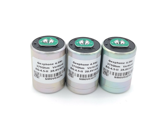
Only 4.5 Hz open-loop geophones should be connected to the E-C111G. Do not connect:
- Geophones with natural frequencies other than 4.5 Hz
- Broadband seismometers or accelerometers
- Force-balance or feedback-based sensors
Even though the inputs are protected against overvoltage and current surges, connecting incompatible high-sensitivity instruments can result in signal distortion, loss of accuracy, or permanent damage to the input circuitry.
For accurate measurements and safety, always ensure the sensor is impedance-matched and within the specified dynamic range.